
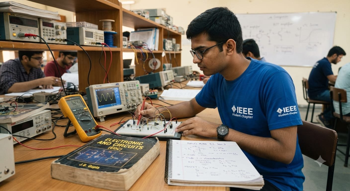
A comprehensive engineering learning guide covering semiconductor fundamentals, electronic devices, circuit operation, numerical problem-solving, university examinations and backlog preparation.
Published by: GATEIIT – Gate Indian Institute of Tutorials
Suggested publication date: 17 November 2026
Content category: Engineering Education | Electronics and Communication Engineering
Reading audience: B.E. / B.Tech students, ECE students, engineering backlog students and electronics learners.
Introduction: Why Is Electronic Devices and Circuits an Important Subject in Engineering?
Electronic Devices and Circuits (EDC) is one of the foundational subjects in electronics-related engineering education. It explains how semiconductor materials behave, how electronic devices operate and how these devices are used to construct functional electronic circuits.
If you are studying B.E. or B.Tech in Electronics and Communication Engineering, Electrical and Electronics Engineering or another branch that includes EDC in its curriculum, understanding this subject can make several advanced engineering subjects easier.
From the diode used in a basic rectifier to the MOSFET used in modern integrated circuits, semiconductor devices are fundamental to electronic technology.
However, many engineering students find EDC challenging because it combines several different areas of learning:
- Semiconductor physics.
- Electrical and electronic circuit fundamentals.
- Mathematical calculations.
- Device characteristics.
- Graphical interpretation.
- Circuit analysis.
- Numerical problem-solving.
- Theoretical derivations.
Students sometimes memorise the operating principles of diodes and transistors without understanding why these devices behave differently under different electrical conditions.
This approach can create problems when they encounter application-based examination questions.
This guide explains Electronic Devices and Circuits systematically, beginning with semiconductor fundamentals and progressing towards diodes, transistors, FETs, MOSFETs and circuit applications.
It also explains how to approach numerical problems, prepare for university examinations and improve performance in a pending EDC subject.
A useful starting point: If you can explain what happens inside a semiconductor when a voltage is applied, understand the operation of a PN junction and analyse the current-voltage characteristics of a transistor, you are building the conceptual foundation needed for much of EDC.
1. What Exactly Do You Study in Electronic Devices and Circuits?
Electronic Devices and Circuits connects the physics of semiconductor materials with the electrical behaviour of electronic components.
A semiconductor material has electrical properties between those of a conductor and an insulator. Its conductivity can be influenced by factors such as doping, temperature and applied electric fields.
By controlling these properties, engineers develop electronic devices capable of controlling current and voltage.
Examples include:
| Electronic device | Primary function |
| PN junction diode | Allows current predominantly in one direction under normal forward and reverse operating conditions |
| Zener diode | Provides voltage regulation in its specified reverse-breakdown operating region |
| BJT | Controls collector current through base-emitter drive |
| JFET | Controls channel current using an electric field |
| MOSFET | Controls channel conduction using an insulated gate |
| LED | Converts electrical energy into light |
| Photodiode | Converts incident light into an electrical response |
These devices are used in power supplies, amplifiers, computers, mobile phones, communication equipment, automotive electronics and semiconductor integrated circuits.
EDC is therefore not simply a theoretical engineering subject. It provides the foundation for understanding how many everyday electronic systems function.
2. Semiconductor Fundamentals: The Foundation of EDC
Before studying electronic devices, it is important to understand semiconductor materials.
2.1 Conductors, Insulators and Semiconductors
Materials can broadly be classified according to their electrical conductivity.
Conductors: Materials such as copper and aluminium allow electric current to flow relatively easily because they have a large number of available charge carriers.
Insulators: Materials such as glass and rubber strongly resist the movement of electric charge under normal conditions.
Semiconductors: Materials such as silicon and germanium have electrical properties between conductors and insulators. Their conductivity can be controlled through doping and other physical mechanisms.
Silicon is particularly important in semiconductor technology because of its electrical properties and suitability for semiconductor manufacturing.
2.2 Energy Band Theory
Energy band theory explains the allowed energy states available to electrons in a solid.
The two important energy bands in introductory semiconductor physics are:
- Valence band.
- Conduction band.
The forbidden energy gap between these bands is called the band gap.
In a semiconductor, the band gap is sufficiently small for charge carriers to be generated through thermal excitation and other mechanisms.
Understanding energy band diagrams helps explain why conductors, insulators and semiconductors behave differently.
2.3 Intrinsic Semiconductors
An intrinsic semiconductor is a pure semiconductor without intentional impurity doping.
In an intrinsic semiconductor under thermal equilibrium, electron and hole concentrations are equal.
Therefore:
n = p = nᵢ
Where:
- n = electron concentration.
- p = hole concentration.
- nᵢ = intrinsic carrier concentration.
When an electron gains sufficient energy to move into the conduction band, it leaves behind a hole in the valence band.
Both electrons and holes contribute to electrical conduction.
2.4 Extrinsic Semiconductors
An extrinsic semiconductor is produced by intentionally introducing suitable impurities into a semiconductor material.
This process is called doping.
There are two important types.
N-type semiconductor
An N-type semiconductor is produced by doping silicon or another suitable semiconductor with donor impurities.
Electrons become the majority carriers, while holes are the minority carriers.
P-type semiconductor
A P-type semiconductor is produced using acceptor impurities.
Holes become the majority carriers, while electrons are the minority carriers.
Understanding N-type and P-type semiconductor formation is essential before studying PN junctions.
2.5 Drift Current and Diffusion Current
Charge carriers move through semiconductor materials in different ways.
Drift current occurs when charge carriers move under the influence of an electric field.
Diffusion current occurs when charge carriers move due to a concentration gradient.
The distinction is particularly important in understanding PN junction operation.
Students should understand the physical meaning of both currents instead of simply memorising their equations.
3. PN Junction Diode: Construction, Working and Characteristics
A PN junction diode is formed by joining P-type and N-type semiconductor regions.
When these two regions are joined, charge carriers diffuse across the junction and recombine.
This creates a depletion region containing immobile ionised charges.
An internal electric field develops across the depletion region, producing a built-in potential barrier.
The operation of a PN junction changes depending on the applied external voltage.
3.1 Unbiased PN Junction
When no external voltage is applied, the junction reaches equilibrium.
The depletion region forms because electrons and holes diffuse across the junction and recombine.
The electric field created by the depletion region opposes further net diffusion.
Under equilibrium conditions, the net current through the junction is zero.
3.2 Forward Bias
In forward bias, the P-side is connected to a higher potential relative to the N-side.
The applied voltage reduces the effective potential barrier and narrows the depletion region.
As the forward voltage increases, the diode current rises rapidly.
For a conventional silicon diode, approximately 0.7 V is often used as a practical forward-voltage approximation in basic circuit calculations.
However, this is not an exact universal switching threshold. The actual forward voltage depends on current, temperature and device construction.
3.3 Reverse Bias
In reverse bias, the P-side is connected to a lower potential relative to the N-side.
The depletion region widens and the potential barrier increases.
Only a small reverse current generally flows before breakdown, provided the device remains within its rated operating conditions.
3.4 Diode Current Equation
The idealised Shockley diode equation is:
I_D = I_S [exp(V_D / (nV_T)) – 1]
Where:
- I_D = diode current.
- I_S = reverse saturation current.
- V_D = voltage across the diode.
- n = ideality factor.
- V_T = thermal voltage.
At room temperature, the thermal voltage is approximately 25.9 mV.
This equation is important for understanding the exponential relationship between diode voltage and current.
Students should also learn when an ideal diode model, constant-voltage model or exponential model is appropriate for a particular problem.
3.5 Diode Characteristics
The current-voltage characteristic of a PN junction diode shows how diode current changes with applied voltage.
Important regions include:
- Forward-bias region.
- Reverse-bias region.
- Breakdown region.
Understanding the characteristic curve helps students answer both theoretical and numerical questions.
4. Zener Diode and Voltage Regulation
A Zener diode is designed to operate in its specified reverse-breakdown region.
When connected appropriately with a series current-limiting resistor, it can maintain an approximately constant voltage across a load over a specified operating range.
The basic principle is used in voltage-reference and regulation circuits.
Students should understand:
- Zener diode construction.
- Reverse characteristics.
- Breakdown voltage.
- Zener current.
- Dynamic resistance.
- Series resistance.
- Load current.
- Power dissipation.
- Regulation conditions.
A common mistake is to assume that a Zener diode can regulate voltage without considering the current-limiting resistor and power rating.
Both are essential for safe and correct circuit operation.
5. Rectifier Circuits: Converting AC into DC
Rectifiers convert alternating current into unidirectional current.
They are commonly used in power supply circuits.
5.1 Half-Wave Rectifier
A half-wave rectifier uses a single diode to allow one half-cycle of the AC input waveform to pass through the load.
During the opposite half-cycle, the diode blocks current under the usual idealised operating assumptions.
Students should understand:
- Input and output waveforms.
- Average output voltage.
- RMS output voltage.
- Ripple factor.
- Rectification efficiency.
- Peak inverse voltage.
For an ideal half-wave rectifier with a sinusoidal input and resistive load:
V_DC = V_m / π
Where V_m is the peak input voltage.
5.2 Full-Wave Rectifier
A full-wave rectifier uses both halves of the input AC waveform.
Common configurations include:
- Centre-tapped full-wave rectifier.
- Bridge rectifier.
An ideal full-wave rectifier produces:
V_DC = 2V_m / π
Here, V_m is the peak voltage of the rectified sinusoidal waveform before accounting for practical diode drops.
5.3 Filters
Rectifier outputs contain ripple.
Filters are used to reduce variations in the output voltage.
Common filter concepts include:
- Capacitor filters.
- Inductor filters.
- LC filters.
- Pi filters.
Students should understand why a capacitor charges near the waveform peaks and discharges through the load between charging intervals.
This physical explanation makes filter-related numerical problems easier to understand.
6. Clipping and Clamping Circuits
Clipping and clamping circuits are important diode applications.
Although the names sound similar, their functions are different.
Clipping circuits
A clipper limits a portion of the input waveform above or below a selected voltage level.
Clamping circuits
A clamper shifts the DC reference level of a waveform while ideally preserving its peak-to-peak value.
Common topics include:
- Positive clipper.
- Negative clipper.
- Biased clipper.
- Positive clamper.
- Negative clamper.
- Voltage multiplier circuits.
A useful study technique is to draw the input waveform first, identify the conducting diode interval and then construct the output waveform.
7. Bipolar Junction Transistor (BJT)
The Bipolar Junction Transistor is an important semiconductor device used for amplification and switching.
A BJT has three terminals:
There are two common types:
- NPN transistor.
- PNP transistor.
The emitter injects charge carriers, the base controls their transport and the collector collects carriers under the appropriate operating conditions.
7.1 BJT Current Relationships
For a transistor:
I_E = I_C + I_B
Where:
- I_E = emitter current.
- I_C = collector current.
- I_B = base current.
In common introductory transistor analysis, current gain in common-emitter configuration is:
β = I_C / I_B
The common-base current gain is:
α = I_C / I_E
The relationship is:
β = α / (1 – α)
These relationships are frequently used in transistor numerical problems.
7.2 BJT Configurations
Three important configurations are:
Common Base (CB)
The base terminal is common to the input and output circuits.
Common Emitter (CE)
The emitter terminal is common to the input and output circuits.
Common Collector (CC)
The collector terminal is common to the input and output circuits.
Each configuration has different input resistance, output resistance, current gain, voltage gain and phase relationships.
Students should prepare comparison tables rather than memorising each configuration independently.
7.3 BJT Operating Regions
The important operating regions include:
Cut-off region: The transistor is effectively switched off under the specified circuit conditions.
Active region: The transistor operates in its normal forward-active region and can be used for amplification.
Saturation region: The transistor is driven into its on-state switching region.
A student should be able to identify the operating region from circuit conditions rather than assume that every transistor operates as an amplifier.
8. Transistor Biasing and DC Load-Line Analysis
Biasing establishes the required DC operating conditions of a transistor.
The operating point is often called the Q-point.
Correct biasing is important because an unsuitable operating point may cause distortion or unstable circuit operation.
Important biasing techniques include:
- Fixed bias.
- Collector-to-base bias.
- Voltage-divider bias.
- Emitter bias.
8.1 Why Is Biasing Important?
Consider a transistor amplifier.
If the operating point is not appropriately selected, the output waveform may be clipped during one or both portions of the signal cycle.
A suitable biasing arrangement helps maintain the required operating region.
8.2 DC Load Line
The DC load line represents the relationship between collector current and collector-emitter voltage for a particular collector circuit.
For a simple common-emitter circuit:
V_CC = I_C R_C + V_CE
This relationship can be rearranged to:
V_CE = V_CC – I_C R_C
The load line helps identify possible operating points.
Students should practise plotting the load line, identifying intercepts and locating the Q-point.
9. Field Effect Transistors (FET)
A Field Effect Transistor is a semiconductor device in which an electric field controls the current through a conducting channel.
Unlike a conventional BJT, a FET is a unipolar device because its channel current is primarily carried by one type of charge carrier.
Two important categories are:
9.1 Junction Field Effect Transistor (JFET)
A JFET has a semiconductor channel controlled by a reverse-biased gate junction.
Types include:
- N-channel JFET.
- P-channel JFET.
Important topics include:
- Working principle.
- Drain characteristics.
- Transfer characteristics.
- Pinch-off voltage.
- Gate-source voltage.
- Drain current.
Students should understand how changing gate-source voltage affects the channel and drain current.
9.2 JFET Characteristics
The drain characteristics show how drain current changes with drain-source voltage for different gate-source voltages.
The transfer characteristic shows the relationship between drain current and gate-source voltage.
For an idealised JFET operating in its applicable region, the Shockley equation is:
I_D = I_DSS (1 – V_GS / V_P)^2
Where:
- I_D = drain current.
- I_DSS = saturation drain current at V_GS = 0.
- V_GS = gate-source voltage.
- V_P = pinch-off voltage using the sign convention appropriate to the device.
Students must use the sign convention specified by the problem rather than substitute magnitudes without checking.
10. MOSFET: Working Principle, Characteristics and Applications
The Metal Oxide Semiconductor Field Effect Transistor is one of the most important semiconductor devices in modern electronics.
MOSFETs are extensively used in integrated circuits, digital systems, power electronics and electronic switching applications.
A MOSFET typically consists of:
- Semiconductor substrate or body.
- Insulating gate dielectric.
The gate is electrically insulated from the channel by a dielectric layer.
This structure allows the electric field generated by the gate voltage to control channel formation and conduction.
10.1 Types of MOSFET
The main types are:
- Enhancement-mode MOSFET.
- Depletion-mode MOSFET.
Each can be implemented as:
- N-channel MOSFET.
- P-channel MOSFET.
10.2 MOSFET Operating Regions
For a simplified long-channel enhancement-mode NMOS model, the important regions include:
Cut-off region
The gate-source voltage is below the threshold voltage under the idealised model, so no strong inversion channel is formed.
Triode or linear region
A conducting channel exists, and the device operates in its linear region under the applicable terminal-voltage conditions.
Saturation region
The channel is pinched off near the drain end under the conventional long-channel model, and the drain current is approximately controlled by gate overdrive voltage.
These concepts are fundamental for analysing MOSFET circuits.
Real devices exhibit non-ideal effects, so the ideal equations should not be treated as universally exact.
11. Difference Between BJT, JFET and MOSFET
This is an important conceptual comparison for engineering examinations.
| Parameter | BJT | JFET | MOSFET |
| Device type | Bipolar | Unipolar | Unipolar |
| Control mechanism | Base current | Electric field | Gate electric field |
| Main terminals | Emitter, Base, Collector | Source, Gate, Drain | Source, Gate, Drain |
| Input characteristics | Generally lower input resistance than FETs | High input resistance | Very high DC gate input resistance in normal operation |
| Gate/base structure | PN junctions | Reverse-biased gate junction | Insulated gate |
| Common applications | Amplifiers and switches | Amplifiers and electronic circuits | Switching, integrated circuits and power applications |
Important: The actual performance of any transistor depends on its device structure, ratings, operating conditions and application. A comparison table is a starting point, not a substitute for studying device characteristics.
12. Important Electronic Devices and Circuits Formulas
Students preparing for examinations should maintain a separate formula notebook.
The following are useful introductory relationships.
| Concept | Formula |
| Semiconductor conductivity | σ = q(nμₙ + pμₚ) |
| Drift current density | Jₙ = qnμₙE |
| Electron diffusion current density | Jₙ,diff = qDₙ(dn/dx) |
| Diode current | I_D = I_S(e^(V_D/nV_T) – 1) |
| BJT emitter current | I_E = I_C + I_B |
| Common-emitter current gain | β = I_C/I_B |
| Common-base current gain | α = I_C/I_E |
| Ideal half-wave rectifier DC output | V_m/π |
| Ideal full-wave rectifier DC output | 2V_m/π |
| Simple collector circuit | V_CC = I_C R_C + V_CE |
| Idealised JFET equation | I_D = I_DSS(1 – V_GS/V_P)² |
The formula sheet should also mention the assumptions behind each equation.
For example, the rectifier output expressions assume ideal diodes and a sinusoidal input with the stated peak voltage.
A common examination mistake is applying a formula without checking its assumptions.
13. Solved EDC Numerical Examples for Engineering Students
The best way to develop confidence in EDC is to solve problems gradually, beginning with simple applications and moving towards more complex circuits.
The following worked examples illustrate the method.
Example 1: Semiconductor Conductivity
Question:
A semiconductor has an electron concentration of 2 × 10²¹ m⁻³ and an electron mobility of 0.14 m²/Vs. Assume hole contribution is negligible.
Calculate its conductivity.
Given:
n = 2 × 10²¹ m⁻³
μₙ = 0.14 m²/Vs
q = 1.6 × 10⁻¹⁹ C
Formula:
σ = qnμₙ
Substitution:
σ = (1.6 × 10⁻¹⁹)(2 × 10²¹)(0.14)
Answer:
σ = 44.8 S/m
This example demonstrates how carrier concentration and mobility influence semiconductor conductivity.
Example 2: BJT Collector Current
Question:
A transistor has a base current of 40 μA and a common-emitter current gain β of 100.
Calculate the collector current.
Given:
I_B = 40 μA
β = 100
Formula:
I_C = βI_B
Substitution:
I_C = 100 × 40 μA
Answer:
I_C = 4 mA
This result assumes the transistor is operating in the forward-active region and is not limited by the collector circuit.
Example 3: BJT Emitter Current
Question:
A transistor has a collector current of 4 mA and a base current of 40 μA. Calculate the emitter current.
Formula:
I_E = I_C + I_B
Substitution:
I_E = 4 mA + 0.04 mA
Answer:
I_E = 4.04 mA
Example 4: Half-Wave Rectifier
Question:
An ideal half-wave rectifier receives a sinusoidal input with a peak voltage of 20 V. Calculate its average output voltage.
Formula:
V_DC = V_m/π
Substitution:
V_DC = 20/3.1416
Answer:
V_DC ≈ 6.37 V
This is the ideal average output. A practical circuit will have additional losses, including the diode forward-voltage drop.
Example 5: Transistor Collector Circuit
Question:
A transistor circuit has a supply voltage of 12 V, collector resistance of 2 kΩ and collector current of 3 mA.
Calculate collector-emitter voltage, assuming a simple resistive collector circuit and neglecting other voltage drops.
Formula:
V_CE = V_CC – I_C R_C
Substitution:
V_CE = 12 – (0.003 × 2000)
V_CE = 12 – 6
Answer:
V_CE = 6 V
The operating-region assumption should still be checked against the transistor’s characteristics and circuit configuration.
14. How to Solve Electronic Devices and Circuits Numericals Correctly
Many students make avoidable mistakes while solving numerical problems.
A systematic method helps.
Step 1: Read the question carefully.
Identify the device, circuit configuration and operating conditions.
Step 2: Write the given quantities.
List all known values with their units.
Step 3: Identify what must be calculated.
Do not start substituting numbers before understanding the requirement.
Step 4: Select the correct formula.
Check the physical assumptions behind the equation.
Step 5: Convert units.
Pay attention to microamperes, milliamperes, kilo-ohms and other prefixes.
Step 6: Substitute values.
Show the calculation clearly.
Step 7: Check the result.
Check units, magnitude and physical feasibility.
Step 8: Interpret the answer.
Where appropriate, check whether the calculated operating point is consistent with the assumed device region.
This method is particularly useful for transistor biasing, diode circuits and semiconductor calculations.
15. Important Diagrams Every EDC Student Should Practise
Diagrams are essential for explaining semiconductor device operation.
Students should practise drawing and interpreting:
- Energy band diagrams of conductors, insulators and semiconductors.
- Intrinsic semiconductor structure.
- N-type and P-type semiconductor structures.
- PN junction under unbiased conditions.
- PN junction under forward bias.
- PN junction under reverse bias.
- Diode V-I characteristics.
- Zener diode characteristics.
- Half-wave rectifier circuit and waveforms.
- Full-wave rectifier circuit and waveforms.
- Clipping and clamping circuits.
- NPN and PNP transistor structures.
- CB, CE and CC transistor configurations.
- BJT input and output characteristics.
- DC load-line diagram.
- Transistor biasing circuits.
- JFET construction and characteristics.
- Enhancement and depletion MOSFET structures.
- MOSFET output and transfer characteristics.
Students should label diagrams correctly and understand what each region or terminal represents.
Simply reproducing a diagram without understanding it may not help when the examination question changes the circuit conditions.
16. How to Prepare for VTU Electronic Devices and Circuits Examinations
VTU students should begin by identifying their exact subject code, scheme and syllabus.
It is important not to assume that every student follows the same EDC syllabus.
Different academic schemes and university programmes may prescribe different topics and assessment patterns.
A practical examination preparation strategy can include the following stages.
Stage 1: Understand the Prescribed Syllabus
Obtain the latest applicable syllabus from the official university source.
Identify:
- Number of units or modules.
- Prescribed topics.
- Important device characteristics.
- Required derivations.
- Numerical problem areas.
- Recommended textbooks.
- Examination pattern.
Stage 2: Build the Fundamentals
Do not begin with complex transistor numerical problems if semiconductor fundamentals are unclear.
Start with:
- Energy bands.
- Intrinsic and extrinsic semiconductors.
- Carrier concentration.
- Drift and diffusion.
- PN junction formation.
Stage 3: Study Each Device Systematically
For every device, learn:
- Working principle.
- Circuit symbol.
- Mathematical equations.
- Operating regions.
- Numerical problems.
This provides a repeatable framework for understanding different devices.
Stage 4: Practise Numerical Problems
Solve problems regularly rather than postponing all numerical practice until the examination week.
Stage 5: Study Previous-Year Questions
Use previous-year question papers to understand how concepts are tested.
Do not assume that a previously repeated question will necessarily appear again.
Stage 6: Take Timed Practice Tests
Practise completing questions within a realistic time limit.
This helps identify whether the difficulty is conceptual understanding, calculation speed or examination presentation.
Stage 7: Revise Weak Chapters
Keep a separate list of mistakes and difficult topics.
Revise these topics more frequently than the chapters you already understand.
17. How to Clear an Electronic Devices and Circuits Backlog
If you have failed EDC, the first step should be to understand why your earlier preparation did not produce the expected result.
Repeating the same study routine without identifying the problem may not be effective.
Consider these questions:
- Did you understand semiconductor fundamentals?
- Could you distinguish forward and reverse bias?
- Were diode circuit numericals difficult?
- Did you understand transistor characteristics?
- Were biasing calculations confusing?
- Did you leave entire units unprepared?
- Did you struggle to finish the examination?
- Did you make mistakes while drawing circuits or writing derivations?
Your answers should determine your preparation strategy.
A Practical Backlog Preparation Framework
First: Identify the weak topics.
List every chapter you cannot confidently explain or solve.
Second: Rebuild conceptual foundations.
Revise the topics that are prerequisites for other chapters.
Third: Solve basic numerical problems.
Start with simple questions and gradually increase complexity.
Fourth: Practise examination-style questions.
Learn to present diagrams, equations and calculations clearly.
Fifth: Take mock examinations.
Use timed practice to assess your progress.
Sixth: Revise repeatedly.
Do not leave revision until the final day.
Students who need additional academic support can enquire about dedicated EDC backlog tuition at GATEIIT.
18. A 30-Day Electronic Devices and Circuits Study Plan
The following schedule is a suggested revision framework for students who already have some familiarity with the subject.
It is not a guaranteed syllabus-completion plan. Students starting from zero may require additional time.
| Days | Topics | Suggested activity |
| 1–3 | Semiconductor fundamentals | Concepts, energy bands, doping |
| 4–5 | Carrier transport | Drift, diffusion and conductivity numericals |
| 6–8 | PN junction diode | Formation, biasing and characteristics |
| 9–10 | Zener diode | Breakdown and regulation problems |
| 11–12 | Rectifiers | Half-wave, full-wave and bridge rectifiers |
| 13–14 | Filters and wave shaping | Clipping, clamping and filter concepts |
| 15–18 | BJT | Construction, configurations and characteristics |
| 19–20 | Transistor biasing | Load lines and numerical practice |
| 21–22 | JFET | Construction and characteristics |
| 23–25 | MOSFET | Types, operating regions and characteristics |
| 26–27 | Formula and diagram revision | Practice important equations and diagrams |
| 28 | Previous-year questions | Solve relevant university questions |
| 29 | Mock examination | Timed examination practice |
| 30 | Final revision | Correct mistakes and revise weak topics |
Recommended Daily Study Routine
A student with approximately three hours available per day could divide the time as follows:
- 60 minutes: Conceptual learning.
- 45 minutes: Numerical problem-solving.
- 30 minutes: Diagrams and derivations.
- 30 minutes: Previous questions or practice problems.
- 15 minutes: Revision of mistakes and formulas.
Consistency is generally more useful than studying for long hours without a clear plan.
19. Common Mistakes Engineering Students Make in EDC
Understanding mistakes is an important part of learning.
Here are some common problems.
Mistake 1: Memorising semiconductor theory without understanding it
Learn how electrons, holes and electric fields contribute to semiconductor behaviour.
Mistake 2: Confusing forward and reverse bias
Always identify the applied voltage polarity before analysing the diode.
Mistake 3: Treating the silicon diode voltage drop as an exact constant
The 0.7 V approximation is useful in basic circuit models but actual diode voltage depends on operating conditions.
Mistake 4: Confusing BJT current gain and voltage gain
β represents common-emitter current gain under the relevant conditions. It is not voltage gain.
Mistake 5: Mixing up transistor configurations
Practise identifying the common terminal before analysing a circuit.
Mistake 6: Ignoring the operating region
Check whether the transistor is in cut-off, active or saturation operation before applying the relevant model.
Mistake 7: Confusing JFET and MOSFET characteristics
Study their construction and gate-control mechanisms separately.
Mistake 8: Memorising equations without assumptions
An equation may only apply under certain operating conditions.
Mistake 9: Avoiding numerical problems
Numerical ability develops through practice, not through reading solved answers alone.
Mistake 10: Studying without checking the prescribed syllabus
Always prepare according to the current scheme applicable to your university and semester.
20. How Is EDC Connected to Other Engineering Subjects?
Electronic Devices and Circuits creates a foundation for several advanced electronics subjects.
| Related subject | Connection with EDC |
| Analog Electronics | Diode and transistor circuit applications |
| Microelectronics | Semiconductor device operation |
| VLSI Design | MOSFETs and integrated circuit devices |
| Digital Electronics | Transistor switching and device behaviour |
| Electronic Circuit Design | Electronic components and circuit analysis |
| Communication Engineering | Amplification and electronic circuit fundamentals |
| Power Electronics | Semiconductor switching devices |
| Embedded Systems | Electronic hardware and semiconductor components |
| Semiconductor Technology | Device physics and fabrication fundamentals |
Students who understand EDC concepts may find it easier to approach these subjects because they already understand some of the underlying electronic device principles.
21. How EDC Concepts Are Used in Real Electronic Technology
It is easier to remember a concept when you understand where it is used.
Example 1: Mobile Phone Chargers
A charger contains power conversion circuitry in which semiconductor devices perform switching, rectification and regulation functions.
Example 2: Computer Processors
Modern processors contain enormous numbers of semiconductor transistors, primarily MOSFET-based devices in CMOS technologies.
Example 3: LED Lighting
Light-emitting diodes convert electrical energy into light through semiconductor processes.
Example 4: Solar Energy Systems
Solar cells use semiconductor junctions to convert incident light into electrical energy.
Example 5: Automotive Electronics
Modern vehicles use semiconductor devices in control units, power conversion, sensing and switching applications.
Example 6: Communication Equipment
Amplifier circuits and semiconductor devices are used throughout communication systems.
These examples show why electronic devices are important beyond university examinations.
22. Useful Learning Resources for Electronic Devices and Circuits
Students should use reliable educational resources alongside their prescribed textbooks.
The following are useful academic resources:
- NPTEL – Basic Electronics
An educational course covering semiconductor materials, PN junction diodes, rectifiers, transistor operation, biasing, MOSFETs and other fundamental topics.
https://nptel.ac.in/courses/117103063
- NPTEL / IISc – Semiconductor Devices and Circuits
A deeper academic resource covering semiconductor physics, PN junctions, BJT, MOS capacitors, MOSFETs and the relationship between device physics and circuit behaviour.
https://nptel.ac.in/courses/108108112
- SWAYAM – Fundamentals of Semiconductor Devices
A useful resource for undergraduate students studying energy bands, doping, carrier statistics, PN junctions, BJTs and MOSFETs.
https://onlinecourses.nptel.ac.in/e-learning/preview/noc25_ee39
- Prescribed University Textbooks
Always refer to the textbooks recommended by your university or faculty.
Different universities may prescribe different books and levels of mathematical depth.
These external resources are supplementary. They should not replace your official syllabus, classroom teaching or examination requirements.
23. When Should You Consider Additional EDC Tuition?
Self-study works well for students who can independently understand concepts, solve numerical problems and maintain a regular preparation schedule.
However, additional teaching support may be useful when:
- You repeatedly struggle with the same chapters.
- You cannot understand semiconductor physics.
- You have difficulty solving transistor numerical problems.
- Your fundamentals are weak.
- You have missed important college classes.
- You have an upcoming supplementary examination.
- You have failed EDC in a previous attempt.
- You need individual doubt-clearing.
- You require a structured preparation timetable.
The purpose of tuition should be to address specific learning gaps rather than simply increase the number of classroom hours.
Electronic Devices and Circuits Tuition at GATEIIT, Bangalore
GATEIIT – Gate Indian Institute of Tutorials provides personalised academic tuition programmes for engineering students.
Students can enquire about Electronic Devices and Circuits tuition for B.E. and B.Tech courses, including:
- Semiconductor physics.
- PN junction diodes.
- Zener diodes and rectifiers.
- BJT and transistor biasing.
- JFET and MOSFET.
- Electronic circuit analysis.
- Numerical problem-solving.
- University semester preparation.
- VTU EDC backlog tuition.
- Supplementary examination preparation.
- One-to-one personal tuition.
Depending on the academic requirement and faculty availability, students can discuss offline, online and small-group learning options.
GATEIIT Centre Address:
3rd Floor, #1743, Sri Raghavendra Plaza,
17th Main Road, JP Nagar 2nd Phase,
Bangalore – 560078, Karnataka, India.
Call: 8884416155
WhatsApp: 8884416154
Official Website: https://www.gateiit.com/
Dedicated EDC Tuition Page:
https://gateiit.com/electronic-devices-and-circuits-tuition-bangalore.html
Google Maps:
https://maps.app.goo.gl/MtzbVkqywCkwKcc4A
Students can share their university, branch, semester, EDC subject code and examination date to enquire about an appropriate preparation programme.
24. Frequently Asked Questions About Electronic Devices and Circuits
Q1. Is Electronic Devices and Circuits difficult for B.E. and B.Tech students?
EDC can be challenging because it combines semiconductor physics, circuit analysis, mathematical calculations and device characteristics. Students who understand the fundamentals before attempting advanced numerical problems generally find the subject easier to approach.
Q2. What are the most important topics in Electronic Devices and Circuits?
Important topics commonly include semiconductor fundamentals, energy band theory, PN junction diodes, Zener diodes, rectifiers, BJT, transistor configurations, biasing, JFET and MOSFET characteristics. The exact importance depends on the applicable university syllabus.
Q3. What should I study first in EDC?
Begin with conductors, insulators, semiconductor materials, energy bands, intrinsic and extrinsic semiconductors, doping, carrier concentration, drift and diffusion. These concepts form the foundation for understanding electronic devices.
Q4. What is the difference between intrinsic and extrinsic semiconductors?
An intrinsic semiconductor is an idealised pure semiconductor without intentional impurity doping. An extrinsic semiconductor has been intentionally doped to modify its electrical properties and carrier concentration.
Q5. Why is a depletion region formed in a PN junction?
When P-type and N-type materials are joined, electrons and holes diffuse across the junction and recombine. This leaves behind immobile ionised charges, producing a region depleted of mobile carriers.
Q6. What happens when a PN junction diode is forward biased?
Forward bias reduces the effective potential barrier and narrows the depletion region, allowing a substantial current to flow as the applied voltage increases.
Q7. What is the difference between a normal diode and a Zener diode?
A normal PN junction diode is commonly used in forward conduction, whereas a Zener diode is specifically designed to operate in its reverse-breakdown region within specified current and power ratings.
Q8. What is the function of a rectifier?
A rectifier converts an alternating electrical input into a unidirectional output. Half-wave and full-wave rectifiers are common introductory circuit configurations.
Q9. What is the difference between a half-wave and full-wave rectifier?
A half-wave rectifier uses one half-cycle of the AC waveform, whereas a full-wave rectifier uses both half-cycles to produce a unidirectional output.
Q10. What are the three configurations of a BJT?
The three main configurations are Common Base, Common Emitter and Common Collector. Each has different electrical characteristics and applications.
Q11. What is transistor biasing?
Transistor biasing establishes the DC operating conditions required for the transistor to function in the intended operating region.
Q12. What is a Q-point?
The Q-point, or quiescent operating point, represents the DC operating condition of a transistor when no input signal is applied.
Q13. What is the difference between BJT and MOSFET?
A BJT is a bipolar device whose collector current is controlled through base-emitter drive, while a MOSFET is a field-effect device whose channel conduction is controlled by the gate electric field.
Q14. What is the difference between JFET and MOSFET?
A JFET controls its channel through a reverse-biased gate junction. A MOSFET uses an insulated gate structure to control channel formation and conduction.
Q15. Is MOSFET important for modern electronics?
Yes. MOSFETs are fundamental to modern integrated circuits, digital processors, memory devices and many power electronic applications.
Q16. How can I improve my EDC numerical problem-solving skills?
Start with basic semiconductor calculations, diode equations, rectifier problems and transistor current relationships. Gradually move towards biasing and device-characteristic problems. Always show the given values, formula, substitution, units and final answer.
Q17. How can I prepare for VTU EDC examinations?
First identify your applicable VTU scheme and official syllabus. Then prepare unit-wise, practise important diagrams and derivations, solve numerical problems and use previous-year question papers for examination practice.
Q18. How can I clear an EDC backlog?
Identify your weak chapters, revise the fundamentals, practise numerical problems and solve relevant previous-year questions. Take timed mock tests and revise mistakes systematically.
Q19. Can I study EDC in 30 days?
A student with prior knowledge may use a 30-day revision plan to revisit important concepts and practise examination questions. A beginner may need more time depending on the syllabus and available study hours.
Q20. Which books are useful for EDC?
Useful references include the prescribed university textbooks and recognised introductory electronics and semiconductor-device textbooks. Students should follow the books recommended for their particular university scheme.
Q21. Is EDC useful for GATE ECE preparation?
Yes. Semiconductor devices, diodes, BJTs, MOSFETs and related circuit concepts can contribute to preparation for relevant GATE ECE topics. However, GATE preparation requires a separate syllabus-oriented approach and additional depth in applicable subjects.
Q22. Where can I find Electronic Devices and Circuits tuition in Bangalore?
Students can enquire about dedicated EDC tuition at GATEIIT, JP Nagar 2nd Phase, Bangalore. One-to-one, small-group and online tuition options can be discussed according to faculty availability.
Q23. Does GATEIIT provide EDC backlog tuition?
Students with pending EDC papers can enquire about subject-wise backlog preparation, including conceptual revision, numerical practice and university examination preparation.
Q24. Can I take only MOSFET or BJT tuition?
Students can enquire about selected-topic tuition for difficult chapters, subject to faculty availability and the teaching programme.
Q25. How do I contact GATEIIT for EDC tuition?
Call 8884416155 or WhatsApp 8884416154. Share your university, engineering branch, semester and subject code to discuss your requirements.
Conclusion: Build Your EDC Fundamentals Before Moving to Advanced Electronics
Electronic Devices and Circuits is an important subject that connects semiconductor physics with practical electronic applications.
A student who understands energy bands, semiconductor doping, PN junction operation, diode characteristics, BJT behaviour, transistor biasing and MOSFET operation develops a strong foundation for further study in electronics engineering.
The most effective way to learn EDC is to combine conceptual understanding with mathematical practice, circuit diagrams, numerical problem-solving and regular revision.
If you are preparing for a university semester examination, working towards clearing an EDC backlog or trying to strengthen your electronics fundamentals, start by identifying the topics you find difficult and preparing a realistic study plan.
Understand the device. Analyse the circuit. Solve the problem. Verify the result.
That is the foundation of effective Electronic Devices and Circuits learning.
For students seeking additional academic support, GATEIIT offers enquiries for personalised Electronic Devices and Circuits tuition in Bangalore and online.
GATEIIT – Gate Indian Institute of Tutorials
JP Nagar 2nd Phase, Bangalore.
Call: 8884416155
WhatsApp: 8884416154
Website: www.gateiit.com
AUTHOR, TECHNICAL REVIEW AND CONTENT TRANSPARENCY
Editorial publisher: GATEIIT – Gate Indian Institute of Tutorials.
Author attribution: GATEIIT Academic Content Team. Use this byline only if the team genuinely takes editorial responsibility for the published article.
Technical reviewer: [Insert the actual name of the EDC / Electronics Engineering faculty member who reviews and approves this article.]
Reviewer qualifications: [Add the reviewer’s genuine engineering degree, postgraduate qualification, relevant subject specialisation and teaching experience, as applicable.]
Author profile: Link the byline to a genuine GATEIIT editorial or author profile explaining the team’s educational content responsibilities and subject coverage.
Content methodology: This educational guide has been organised around undergraduate-level semiconductor and electronic-device concepts, with worked introductory calculations, practical learning examples and examination preparation guidance. Technical content should be checked against recognised academic resources and the student’s applicable university syllabus before publication.
Originality and editorial responsibility: The publisher should verify formulas, numerical examples, diagrams, references and syllabus-specific claims before release. AI-assisted drafting, if used, must receive genuine human editorial and technical review. No artificial author credentials or unsupported teaching-experience claims should be added.
Last reviewed: Update this field only after a genuine technical review.
Next review: Review when relevant university syllabi, examination schemes, academic references or material technical explanations change.
REFERENCES AND FURTHER READING
- NPTEL – Basic Electronics, IIT Guwahati: https://nptel.ac.in/courses/117103063
- NPTEL – Semiconductor Devices and Circuits, IISc Bangalore: https://nptel.ac.in/courses/108108112
- SWAYAM – Fundamentals of Semiconductor Devices: https://onlinecourses.nptel.ac.in/e-learning/preview/noc25_ee39
- Relevant university-prescribed EDC textbooks and officially published syllabi.
- Official manufacturer datasheets and semiconductor device application notes when discussing device-specific electrical characteristics.