
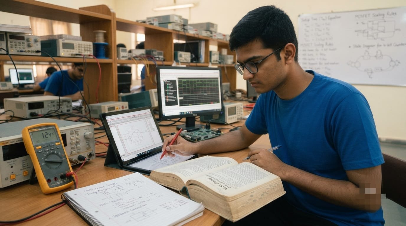
If you have failed VLSI Design in your BE/BTech examination, have a pending backlog or are preparing for a supplementary or repeater examination, the first thing you should do is stop studying randomly. Begin with your university syllabus, identify the topics you do not understand, check the examination pattern and create a realistic plan for completing the subject.
VLSI Design becomes difficult for many engineering students because it combines semiconductor device concepts, MOSFET operation, CMOS logic, circuit characteristics, numerical problem-solving and fabrication processes. Simply reading the textbook repeatedly may not be enough. You need to understand the underlying concepts, practise relevant questions and learn how to present your answers clearly in the examination.
This guide explains how BE, BTech and MTech students can prepare for a VLSI supplementary examination systematically, whether they have two weeks, one month or more time available.
It is especially useful for students who:
- Have failed VLSI Design in a previous semester.
- Have a VLSI backlog or year back.
- Are appearing for a supplementary or repeater examination.
- Understand some topics but cannot solve numerical problems.
- Have difficulty with CMOS inverter characteristics and MOSFET operation.
- Have studied the subject before but cannot remember the concepts.
- Need to restart VLSI preparation after a long academic gap.
One important point: VLSI subject names, module arrangements, marks distribution and prescribed topics differ between universities and academic regulations. Always use your current official syllabus and examination scheme as the final reference. The topic suggestions in this article are a preparation framework, not a universal list of questions guaranteed to appear in an examination.
1. Why do engineering students fail VLSI Design?
Before preparing again, understand why the previous attempt did not go well. If you repeat the same study method, you may repeat the same mistakes.
In many cases, the problem is not that the student cannot understand VLSI. The problem is that several connected concepts were never understood properly.
Reason 1: Weak understanding of semiconductor fundamentals
VLSI depends on the behaviour of semiconductor devices. Students who are uncomfortable with basic semiconductor concepts may find MOSFET operation, transistor characteristics and CMOS circuit behaviour difficult.
For example, if you cannot distinguish the operating regions of a MOSFET, questions involving drain current and device behaviour can become confusing.
Reason 2: Memorising MOSFET equations without understanding them
Students sometimes memorise equations but do not understand:
- What each parameter represents.
- Which operating condition applies.
- What assumptions are used in a particular equation.
- Which values are given in the question.
- Whether the final answer is physically reasonable.
This makes numerical problems unnecessarily difficult.
Reason 3: Difficulty understanding CMOS circuits
CMOS inverter operation is a foundational topic in many VLSI syllabuses. Students may remember the diagram but struggle to explain what happens when the input voltage changes.
They may also confuse the operation of NMOS and PMOS transistors or fail to explain the voltage transfer characteristics.
Reason 4: Not practising circuit diagrams
VLSI answers often require properly drawn and labelled circuit diagrams, transistor connections, characteristic curves, fabrication sequences or logic structures.
Reading an explanation without practising the corresponding diagram can leave students unprepared to reproduce it during an examination.
Reason 5: Studying without checking the university syllabus
A student may spend several hours studying advanced industry-oriented VLSI topics while leaving prescribed university modules incomplete.
For backlog preparation, the priority is to complete the subject that the university will examine—not to cover every topic in the semiconductor industry.
Reason 6: Starting previous-year question papers too late
Some students read the entire textbook before attempting even one university question paper. As a result, they discover their weaknesses only a few days before the examination.
Previous-year questions should be used during preparation, not just on the final day.
Reason 7: Poor answer presentation
A student may understand a concept but lose marks because the answer is incomplete, disorganised or missing a required circuit diagram, derivation, labelled figure or explanation.
A correct concept must also be communicated clearly.
2. First understand which VLSI subject you actually need to clear
Before beginning preparation, confirm the exact subject name and subject code printed in your university records.
The term VLSI may refer to different subjects, including:
| Subject name | Typical academic focus |
| VLSI Design | MOS devices, CMOS circuits and integrated-circuit design fundamentals |
| CMOS VLSI Design | CMOS logic, inverter characteristics, power, delay and circuit design |
| VLSI Technology | Semiconductor fabrication and manufacturing processes |
| Digital VLSI Design | Digital circuits and their VLSI implementation |
| Analog VLSI Design | MOS-based analog circuits and amplifier fundamentals |
| VLSI Circuits and Systems | Circuit and system-level concepts |
| Advanced VLSI Design | More specialised design topics, depending on the university |
Do not assume that the syllabus of VLSI Design is identical to CMOS VLSI Design or VLSI Technology.
Before studying, collect these four documents:
- The latest applicable university syllabus.
- The subject code and academic regulation.
- The examination question-paper pattern, if published.
- Previous-year question papers for the same or comparable syllabus.
If you are a VTU student, check the syllabus applicable to your admission year and academic regulation. Students from autonomous colleges should use their own institution’s curriculum.
3. How to identify the most important VLSI topics for your examination
Students frequently search for a list of important VLSI questions. Such lists can be useful for revision, but relying on them alone is risky.
A better method is to classify the syllabus into three groups.
Group A: Topics you understand reasonably well
These are topics you can explain without continuously referring to notes. Revise them and practise examination questions so that you do not lose marks through careless mistakes.
Group B: Topics you partly understand
You may know the definitions but struggle with circuit diagrams, derivations or numerical problems. These topics need focused teaching and practice.
Group C: Topics you do not understand
These are your highest-priority learning areas. Start with the prerequisites and build the concept step by step.
Use the following tracker:
| Topic | Current understanding | Preparation action |
| Semiconductor fundamentals | Strong / Partial / Weak | Revise or rebuild basics |
| MOSFET operation | Strong / Partial / Weak | Study operating regions and characteristics |
| CMOS inverter | Strong / Partial / Weak | Practise operation and VTC |
| CMOS logic gates | Strong / Partial / Weak | Draw and analyse circuits |
| Power and delay | Strong / Partial / Weak | Understand equations and solve problems |
| VLSI fabrication | Strong / Partial / Weak | Learn process sequence and diagrams |
| Layout and design rules | Strong / Partial / Weak | Practise syllabus-specific diagrams |
| Other prescribed modules | Strong / Partial / Weak | Follow the official syllabus |
This simple exercise prevents you from spending too much time revising topics you already know while ignoring the subjects responsible for your previous failure.
4. VLSI topics that deserve focused preparation
The following areas are commonly found in VLSI-related engineering curricula. Select only the topics included in your own syllabus.
A. Semiconductor and MOSFET fundamentals
Start with the device concepts required for understanding VLSI circuits.
Study:
- Basic semiconductor concepts.
- Intrinsic and extrinsic semiconductors, where prescribed.
- PN junction fundamentals, where relevant.
- MOS capacitor fundamentals, where prescribed.
- NMOS and PMOS transistor structure.
- MOSFET operating regions.
- Threshold voltage.
- Drain current characteristics.
- Transfer and output characteristics.
- Channel-length modulation, if included.
- Body effect, if included.
How to prepare this section:
Do not merely memorise the names of the MOSFET operating regions. Understand the conditions that determine each region and how the transistor behaves under those conditions.
Practise drawing the device structure and characteristic curves. Work through numerical examples using the equations and assumptions specified in your course material.
B. CMOS inverter
The CMOS inverter is one of the most useful circuits for understanding basic CMOS operation.
Prepare:
- CMOS inverter circuit diagram.
- NMOS and PMOS connections.
- Working when input is LOW.
- Working when input is HIGH.
- Voltage transfer characteristics.
- Switching threshold.
- Noise margins.
- Static power considerations.
- Dynamic switching behaviour.
- Propagation delay, if prescribed.
A useful self-test:
Can you draw a CMOS inverter without looking at your notes?
Can you explain why one transistor is conducting while the other is off for the two steady-state input conditions?
Can you explain how the output changes as the input voltage changes?
If you cannot answer these questions, revise the circuit before moving to more complicated CMOS gates.
C. CMOS logic gates
Students should understand how logic functions are implemented using transistor networks.
Depending on the syllabus, practise:
- CMOS NAND gate.
- CMOS NOR gate.
- Complex logic gates.
- Pull-up network.
- Pull-down network.
- Series and parallel transistor arrangements.
- Logic expressions and circuit implementation.
Do not learn each circuit as an isolated picture. Understand how the required logic function determines the arrangement of the transistor networks.
D. Power dissipation and delay
This section can involve both theory and numerical questions.
Topics may include:
- Static power dissipation.
- Dynamic power dissipation.
- Switching activity.
- Load capacitance.
- Supply voltage.
- Propagation delay.
- Rise time and fall time.
- Delay-related circuit parameters.
How to practise numerical problems:
- Write down the given values.
- Identify the quantity being asked.
- Write the relevant equation.
- Check the assumptions behind that equation.
- Substitute values carefully.
- Maintain consistent units.
- Show the calculation steps.
- Check whether the answer is reasonable.
Avoid writing an equation simply because it appears in your formula sheet. Make sure it applies to the situation described in the question.
E. VLSI fabrication technology
If fabrication is part of your syllabus, prepare the sequence and purpose of the major processes.
Possible topics include:
- Wafer preparation.
- Ion implantation
- Semiconductor process integration.
- CMOS fabrication sequence.
A better way to remember fabrication:
Instead of memorising a disconnected list of processes, understand what each step is intended to achieve.
For every process, prepare four points:
- What is the process?
- Why is it required?
- What happens to the wafer or material?
- What is the result of that process?
Draw a process flow diagram where appropriate. This makes revision easier and helps you organise long answers.
F. Layout and design fundamentals
If included in your syllabus, revise:
- Stick diagrams.
- Layout representation.
- Design rules.
- Basic layout concepts.
- Transistor sizing.
- Area and design considerations.
Practise the diagrams yourself. Merely recognising a layout in a textbook is not the same as being able to reproduce it in an examination.
5. How to solve VLSI numerical problems without getting confused
Numerical problems are often a major source of difficulty for students who have a VLSI backlog.
The most effective way to improve is to use a consistent solving method rather than trying to remember the final answer to every problem.
The eight-step numerical method
Step 1: Read the complete question.
Identify the circuit, transistor type, given parameters and required quantity.
Step 2: Draw the circuit if necessary.
A simple circuit sketch can prevent mistakes in interpreting the question.
Step 3: Write the known values.
For example, list the relevant supply voltage, threshold voltage, device parameters and dimensions provided in the question.
Step 4: Identify the operating condition.
Determine the applicable operating region or circuit condition before selecting an equation.
Step 5: Select the correct equation.
Use the equation prescribed by your textbook or course notes, with its stated assumptions.
Step 6: Substitute values carefully.
Pay attention to units, powers of ten and device dimensions.
Step 7: Show intermediate steps.
Avoid jumping directly from the question to the final answer.
Step 8: Check the result.
Check units, sign, magnitude and whether the result is consistent with the assumptions.
Example of how to approach a MOSFET numerical
Suppose a question provides a MOSFET’s terminal voltages and asks you to identify its operating region.
Do not immediately substitute values into a current equation.
First:
- Identify the transistor type.
- Establish the relevant terminal-voltage differences.
- Determine the threshold condition.
- Check the conditions for the operating regions using the model taught in your syllabus.
- State the region and explain why the conditions are satisfied.
Only after identifying the operating region should you use the appropriate current relationship, if the question asks for current.
This method is more reliable than trying to memorise a collection of unrelated solved examples.
6. How to use previous-year VLSI question papers properly
Previous-year question papers are valuable, but students should use them intelligently.
A question repeated in the past is not guaranteed to appear in the next examination. Likewise, a topic that was not asked recently should not automatically be ignored.
Use previous-year papers to understand:
- The style of university questions.
- The way questions are framed.
- The expected depth of explanations.
- The balance between theory and numerical problems.
- The use of diagrams and derivations.
- The examination’s module-wise coverage, where applicable.
- The amount of time required to complete the paper.
The three-round question-paper method
Round 1: Topic identification
Read the papers and identify which syllabus concepts are being tested. Group similar questions together.
Round 2: Independent solving
Attempt the questions without looking at the answers. Mark the questions you cannot complete.
Round 3: Timed practice
After completing the relevant syllabus, attempt a full paper under the examination’s actual time conditions.
Maintain a separate notebook for mistakes. Write down not just the correct answer, but why your original approach was wrong.
This mistake notebook can become one of your most useful revision resources.
7. A practical 14-day VLSI supplementary examination study plan
A two-week plan may be suitable for students who have already attended classes, possess basic familiarity with the subject and need structured revision.
It is not a guarantee that the complete syllabus can be learnt from scratch in 14 days. Students with substantial conceptual gaps should allow more time or seek additional teaching.
| Day | Suggested focus | What to complete |
| 1 | Syllabus and preparation assessment | Identify weak modules, collect papers and make a topic list |
| 2 | Semiconductor and MOSFET basics | Revise device structure and operating principles |
| 3 | MOSFET characteristics | Practise operating regions and relevant numericals |
| 4 | CMOS inverter | Draw, explain and revise voltage transfer characteristics |
| 5 | CMOS logic gates | Practise NAND, NOR and syllabus-specific logic circuits |
| 6 | Power and delay | Revise equations, assumptions and numerical problems |
| 7 | First revision test | Attempt questions from the topics studied |
| 8 | VLSI fabrication | Revise process steps and draw relevant flow diagrams |
| 9 | Layout and design topics | Practise prescribed diagrams and concepts |
| 10 | Remaining syllabus modules | Complete topics not yet covered |
| 11 | Previous-year question paper | Attempt a paper and identify gaps |
| 12 | Weak-topic correction | Relearn and practise the topics where mistakes occurred |
| 13 | Full examination practice | Attempt a timed paper |
| 14 | Final revision | Review formulae, diagrams, derivations and mistake notebook |
Adjust this plan to your official examination timetable and syllabus. If your subject contains different modules, replace the suggested topics with those prescribed by your university.
What should you do if you have only seven days?
A seven-day schedule should be treated as an emergency revision plan, not a substitute for complete preparation.
- Day 1:Check the syllabus, identify weak topics and organise study material.
- Day 2:Revise the most difficult device and circuit fundamentals.
- Day 3:Practise prescribed numerical problems and circuit diagrams.
- Day 4:Cover the remaining high-priority syllabus modules.
- Day 5:Solve previous-year questions and review mistakes.
- Day 6:Attempt a timed practice paper and correct weak areas.
- Day 7:Revise formulas, diagrams and important concepts; avoid starting an unnecessarily large new topic at the last minute.
If you have not studied VLSI before, seven days may be insufficient for full syllabus preparation. Be realistic about what can be completed.
8. How much time should you study every day?
There is no single daily study duration that works for every student. Your available time, current understanding and examination date matter.
A useful starting routine for a student preparing alongside college or other responsibilities is:
| Study session | Suggested time | Activity |
| Session 1 | 45–60 minutes | Learn one difficult concept |
| Session 2 | 45–60 minutes | Work through solved examples |
| Session 3 | 45 minutes | Solve questions independently |
| Session 4 | 20–30 minutes | Revise earlier topics and mistakes |
Take short breaks between sessions. The goal is not to sit with a textbook for many hours; it is to understand and solve questions independently.
For every topic, try to move through three stages:
Understand → Practise → Recall
If you can explain the topic without looking at the notes and solve a representative question independently, you are making meaningful progress.
9. How to write better answers in a VLSI university examination
Even good preparation can be undermined by poor answer presentation.
The appropriate format depends on the question, but the following approach is useful.
For a theory question
- Begin with a direct definition or introduction.
- Explain the working principle.
- Include a labelled diagram if relevant.
- Explain important stages or operating conditions.
- Add the relevant equations, where required.
- End with the result or application, if appropriate.
For a circuit question
- Draw the circuit clearly.
- Label the input, output and relevant terminals.
- Explain the operation.
- Show the required logic or voltage conditions.
- Include the relevant characteristics if asked.
For a numerical question
- Write the given data.
- State the equation and assumptions.
- Substitute values with units.
- Show intermediate calculations.
- Write the final answer clearly.
For a fabrication-process question
- Explain the purpose of the process.
- Describe the steps in the correct sequence.
- Draw a suitable diagram or flowchart where relevant.
- Mention the resulting structure or outcome.
Do not add irrelevant material simply to make an answer longer. Focus on what the question actually asks and follow the marks allocation and answer expectations of your university.
10. Common mistakes VLSI repeater students should avoid
If you have already failed once, your next attempt should be based on a better method.
Avoid these mistakes:
- Studying only predicted questions.
Predictions are not guarantees. Cover the syllabus and use previous-year questions as practice. - Ignoring basic electronics.
A weak understanding of MOSFET fundamentals can make advanced CMOS topics much harder. - Memorising equations without conditions.
An equation must be used with the correct assumptions and operating conditions. - Reading without drawing.
Practise circuit diagrams, characteristics and fabrication sequences by hand. - Leaving numerical problems until the final week.
Numerical ability improves through repeated practice. - Using notes from a different syllabus.
Check the subject code and academic regulation before relying on another student’s material. - Spending too much time on one difficult topic.
Set a reasonable time limit, identify the exact conceptual gap and seek help if necessary. - Not attempting a timed paper.
Knowing the answers and completing an examination paper within the allotted time are different skills. - Avoiding revision.
Topics studied early can be forgotten if they are not revisited. - Assuming one more attempt will automatically be easier.
A successful repeat attempt requires a change in preparation strategy, not just more hours of reading.
11. What if you have failed VLSI Design more than once?
Students who have attempted the same subject multiple times should not simply repeat the previous preparation routine.
Start by identifying the reason for the repeated difficulty.
| Previous difficulty | What to change in the next attempt |
| Unable to understand basic concepts | Rebuild prerequisites with guided explanations |
| Cannot solve MOSFET numericals | Practise step-by-step problem solving |
| Forget circuit diagrams | Draw circuits regularly without referring to notes |
| Incomplete syllabus | Create a module-wise completion schedule |
| Poor examination time management | Attempt timed question papers |
| Confusion between different equations | Prepare a formula sheet with conditions and assumptions |
| Difficulty writing long answers | Practise structured, syllabus-relevant answers |
| No regular revision | Use short, repeated revision sessions |
If you are unsure where you are going wrong, ask a faculty member to review a previous answer paper, where available, and identify the areas that need improvement.
A useful diagnostic exercise is to attempt a short test covering the main topics of your syllabus without referring to notes. The result can help identify whether your main problem is conceptual understanding, numerical practice, recall or answer presentation.
12. Should you study VLSI alone or take tuition?
Self-study can work well for students who already understand the basics, have good study material and can solve university questions independently.
However, additional teaching may be useful when:
- You have repeatedly failed the same subject.
- You cannot understand MOSFET or CMOS concepts from textbooks.
- You are unable to identify the correct method for numerical problems.
- You have a short preparation window.
- Your syllabus is incomplete.
- You need someone to explain difficult circuit diagrams.
- You require a structured revision and question-practice schedule.
The decision should depend on your actual difficulty, not on the assumption that every backlog student must join coaching.
How personalised VLSI tuition can help
A subject-focused tuition programme can help a student:
- Identify the concepts responsible for repeated mistakes.
- Understand the prescribed syllabus module by module.
- Work through numerical examples with explanations.
- Practise circuit diagrams and derivations.
- Review university question papers.
- Revise weak areas before the examination.
The value of tuition is not simply the number of hours spent in class. It is whether the student becomes capable of solving questions independently.
13. VLSI backlog and supplementary tuition at GATEIIT, Bangalore
Students who need additional academic support can enquire about VLSI subject tuition at GATEIIT.
GATEIIT’s VLSI backlog tuition programme is intended for BE/BTech and MTech students who need help with university-level VLSI subjects, including VLSI Design, CMOS VLSI Design and VLSI Technology, subject to the student’s syllabus and faculty availability.
The tuition plan can be discussed according to:
- University and academic regulation.
- Engineering branch and semester.
- VLSI subject code.
- Number of modules pending.
- Previous examination performance.
- Supplementary examination date.
- Required number of teaching hours.
Available tuition formats
Students can enquire about:
- 10-hour VLSI quick revision.
- 15-hour important-topic tuition.
- 20-hour supplementary crash course.
- 30-hour complete subject tuition.
- 40-hour tuition with additional question practice.
- 50-hour repeater special programme.
- 60-hour one-to-one intensive tuition.
Proposed indicative VLSI tuition fees
| Package | Duration | Proposed fee |
| Quick Revision | 10 hours | ₹3,000 |
| Important Topics Tuition | 15 hours | ₹4,000 |
| Supplementary Crash Course | 20 hours | ₹5,000 |
| Complete Subject Tuition | 30 hours | ₹7,000 |
| Complete Tuition + Question Practice | 40 hours | ₹9,000 |
| Repeater Special Programme | 50 hours | ₹11,000 |
| One-to-One Intensive Tuition | 60 hours | ₹15,000 |
These are proposed indicative package prices, not a confirmation of currently approved GATEIIT fees. Final fees, faculty availability, teaching mode and course duration should be confirmed before enrolment.
Online and classroom tuition
Students can enquire about online classes or classroom tuition at GATEIIT’s JP Nagar centre in Bangalore. One-to-one and small-group formats may be arranged depending on faculty availability and syllabus compatibility.
GATEIIT – Gate Indian Institute of Tutorials
3rd Floor, #1743, Sri Raghavendra Plaza,
17th Main Road, JP Nagar 2nd Phase,
Bangalore – 560078, Karnataka.
Call: 8884416155
WhatsApp: 8884416154
Website: www.gateiit.com
VLSI backlog tuition page: https://gateiit.com/vlsi-subject-tuition-backlog-bangalore.html
Google Maps: https://maps.app.goo.gl/MtzbVkqywCkwKcc4A
14. Frequently Asked Questions about VLSI supplementary examination preparation
1. How can I pass VLSI Design in my supplementary examination?
Start with the applicable university syllabus, identify weak topics, rebuild the necessary fundamentals, practise numerical problems and circuit diagrams, and solve previous-year question papers. Use a realistic timetable and revise regularly.
2. How many days are required to prepare for a VLSI backlog examination?
It depends on your existing understanding and syllabus. A student who has previously studied the subject may use a 14-day revision plan. A student starting from the basics may require several weeks or more.
3. Which topics should I study first in VLSI Design?
Begin with the foundational topics prescribed in your syllabus. These may include semiconductor fundamentals, MOSFET operation, CMOS inverter characteristics and CMOS logic. Then move to numerical problems, power and delay, fabrication and other prescribed modules.
4. Is MOSFET important for VLSI Design examinations?
MOSFET fundamentals are central to many VLSI and CMOS courses. Students should understand transistor structure, operating regions and characteristics wherever these topics are included in their syllabus.
5. How do I prepare for CMOS inverter questions?
Learn the circuit connections, understand the operation for different input conditions, practise the voltage transfer characteristics and revise switching and noise-margin concepts if prescribed.
6. How can I remember VLSI fabrication processes?
Understand the purpose and sequence of each process rather than memorising names alone. Prepare a flowchart and practise explaining what happens during oxidation, lithography, etching, diffusion, implantation and other syllabus-specific steps.
7. Can I pass VLSI by studying only previous-year question papers?
Previous-year papers are useful for understanding question styles and practising concepts. However, depending only on repeated questions is risky because future examination questions may be different.
8. What should I do if I cannot solve VLSI numerical problems?
Start by revising the relevant device or circuit concept. Learn what the variables represent, understand the equation’s assumptions, work through solved examples and then attempt similar problems independently.
9. Is VLSI Design more difficult than other ECE subjects?
Difficulty varies from student to student. Students who are uncomfortable with semiconductor devices, MOSFET characteristics and circuit analysis may find VLSI challenging. A strong foundation and regular problem practice can make the subject easier to understand.
10. Can I prepare for VLSI in 15 days?
Fifteen days may be sufficient for focused revision if you have already studied most of the syllabus. If you have major conceptual gaps or have not completed the subject, you may need more time.
11. How should a repeater student prepare differently?
A repeater should first identify why the previous attempt was unsuccessful. The next plan should directly address weak concepts, numerical problem-solving, incomplete modules, answer presentation or time management.
12. Can I take tuition only for difficult VLSI modules?
Students can enquire about selected-topic tuition, depending on faculty availability and the topics required. This may be useful if most of the syllabus has already been completed.
13. Does GATEIIT provide VLSI backlog tuition in Bangalore?
Students can enquire about VLSI subject tuition at GATEIIT’s JP Nagar centre. Online tuition options may also be available, subject to scheduling and faculty availability.
14. What is the fee for VLSI supplementary tuition at GATEIIT?
Proposed indicative packages start at ₹3,000 for 10 hours, ₹5,000 for 20 hours and ₹7,000 for 30 hours. Confirm the current fee and available teaching arrangements directly with GATEIIT.
15. Can VTU students join VLSI backlog tuition?
Students from VTU-affiliated colleges can enquire. They should provide their applicable academic regulation, subject code and syllabus so that the tuition can be planned correctly.
16. Does GATEIIT guarantee that I will clear my VLSI backlog?
No institute can honestly guarantee a university examination result. Tuition can provide teaching, practice and revision support, but the outcome depends on the student’s preparation, attendance, independent practice and examination performance.
15. Final advice: Do not repeat the same preparation method
A VLSI backlog can feel frustrating, particularly when it delays your semester progression or graduation. But preparing again does not have to mean starting with the same confusion.
First, identify the exact syllabus. Then understand which concepts are weak, learn the fundamentals, practise numerical problems and diagrams, and use previous-year papers to test your preparation. Leave enough time for revision and timed practice.
If you have failed VLSI more than once, do not assume that reading the same notes again will solve the problem. Find out exactly where your understanding breaks down and change your approach.
A well-planned preparation strategy, consistent practice and appropriate academic support can help you approach your next examination with greater clarity and confidence.
Need help preparing for your VLSI supplementary or repeater examination?
Students can contact GATEIIT to discuss their university syllabus, pending modules and suitable VLSI subject tuition options.
Call 8884416155 | WhatsApp 8884416154
GATEIIT – Gate Indian Institute of Tutorials
JP Nagar 2nd Phase, Bangalore – 560078
www.gateiit.com